- 您现在的位置:买卖IC网 > Sheet目录1994 > DS3105LN+ (Maxim Integrated Products)IC TIMING LINE CARD 64-LQFP
DS3105
114
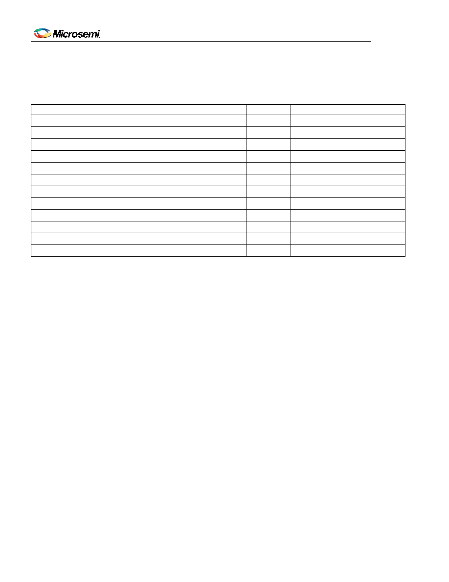
10.4 SPI Interface Timing
Table 10-10. SPI Interface Timing
PARAMETER (Note 1)
SYMBOL
MIN
TYP
MAX
UNITS
SCLK Frequency
fBUS
6
MHz
SCLK Cycle Time
tCYC
100
ns
CS Setup to First SCLK Edge
tSUC
15
ns
CS Hold Time After Last SCLK Edge
tHDC
15
ns
SCLK High Time
tCLKH
50
ns
SCLK Low Time
tCLKL
50
ns
SDI Data Setup Time
tSUI
5
ns
SDI Data Hold Time
tHDI
15
ns
SDO Enable Time (High-Z to Output Active)
tEN
0
ns
SDO Disable Time (Output Active to High-Z)
tDIS
25
ns
SDO Data Valid Time
tDV
50
ns
SDO Data Hold Time After Update SCLK Edge
tHDO
5
ns
Note 1:
All timing is specified with 100pF load on all SPI pins.
发布紧急采购,3分钟左右您将得到回复。
相关PDF资料
DS3106LN+
IC TIMING LINE CARD 64-LQFP
DS3231MZ+
IC RTC I2C 8SOIC
DS3231SN#T&R
IC RTC W/TCXO 16-SOIC
DS3232MZ+
IC RTC W/SRAM I2C 8SOIC
DS3232SN#T&R
IC RTC W/TCXO 20-SOIC
DS3234S#
IC RTC W/TCXO 20-SOIC
DS32C35-33#T&R
IC RTC ACCURATE I2C 3.3V 20-SOIC
DS3911T+
IC DAC 10BIT I2C QUAD 14TDFN
相关代理商/技术参数
DS3106
制造商:MAXIM 制造商全称:Maxim Integrated Products 功能描述:Line Card Timing IC
DS3106A10SL3S(621)
制造商:Amphenol Corporation 功能描述:
DS3106A14S2S
制造商:Amphenol Corporation 功能描述:
DS3106A14S2S(621)
制造商:Amphenol Corporation 功能描述:
DS3106A14S5P
制造商:Amphenol Corporation 功能描述:
DS3106A14S5P(621)
制造商:Amphenol Corporation 功能描述:
DS3106A14S5S(621)
制造商:Amphenol Corporation 功能描述:
DS3106A14S6P
制造商:Amphenol Corporation 功能描述: